Electronics Production//
Designing an in-circuit programmer
The first step was to study and understand how an in-circuit works. After studing previous students i chose to procced with the usb-Microchipprogrammer of Valentine since his "idea of this modification is, that the design should be useable without any past assembly soldering. Being new, the USB dose not work and the firmware need to be written to the attiny. Therefore the USB connector is blocked and the ISP is in programing mode. Once the ISP has its firmware, the USB blocking can be snaped of and all circuits needed for programming are gone too. The board is now a USB-ISP device." Valentine
Modifying the original file into a personal one
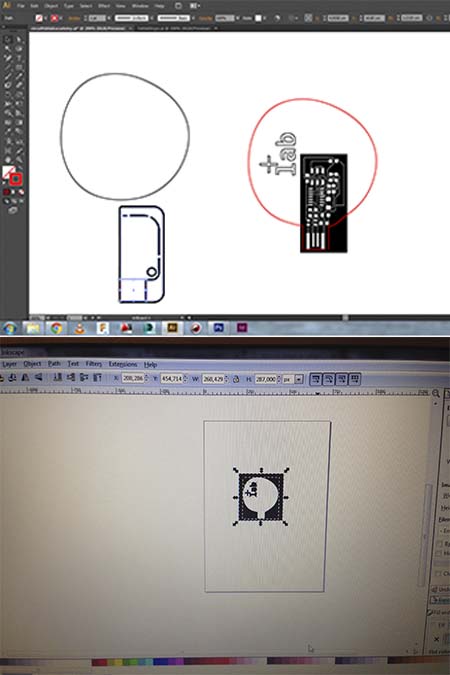
After downloading the png files from the website of Valentine, i decided to modify the outline file and add my fablab's page logo on it. The reason i chose to do it it was because i wanted to make it more personal and because i need something of bigger size in order not to loose it. The software i used was first illustrator, but i faced many problems with export it since fabmodules.org read only files saved in dpi and i wasn't able to change it form ppi into dpi. After i transfered my file into inskape ,i traced the origonal image, i added my design and i worked on the right resolution, the right dpi and forming the right outline for my design.
Preparing the file for the milling machine
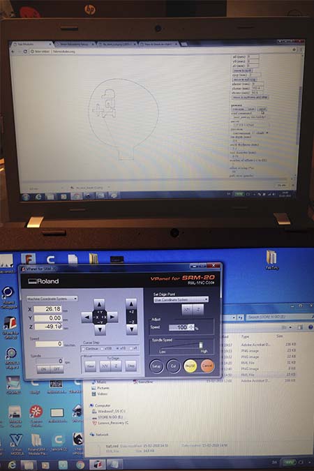
The final png files (the trace file and the outline one) were imported into the fabmodules.org (twice since they are two different procedures, trace and outline cut) were was controlled the machine type (roland milling machine) speed (4), the borders of the cut(0,0), the dpi(1000) and was calculated the procedure. After, the two files were imported into the softwarwe of the Roland machine were the x,y,z axis were set , in the software and on the copper plate. It is very important to follow the exact procedure of setting the right x,y,z axis.
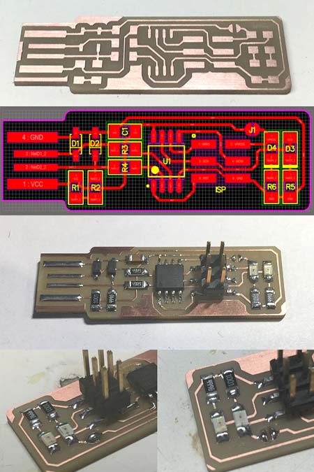
Milling the usb-Microchipprogrammer
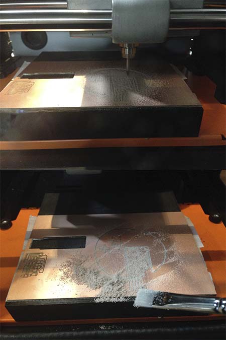
The first step wasafter the control of the right parameters and the preparation of the machine (chooce the right bit for ingraving and cutting, 1/64 inch bit fro engraving and 1/32 inch bit for cutting through) and set the x,y,z axis the attiny were placed after was sticked with double face tape on the wooden plate. It is essentila that the plate is not bend since this will affect the egraving depth. In the egraving file were also placed traces for the outline file in order to be able to control manually the right position of the cut out file in case something was wrong. The ouline was also engraved and the was cut out after with the cut out file. It is also essential to remove the dust, gently by usinga bruch , before the cut out will start.
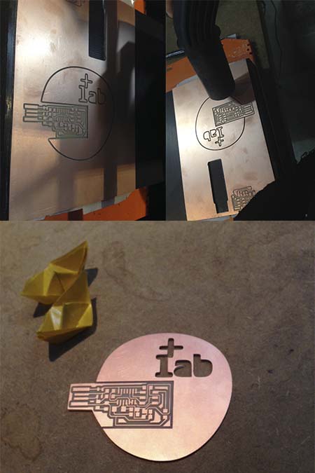
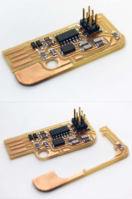
The final- product
The outline file were cut out exactly to the engraved outline path (after changing the engraving bit inti the right cutting bit) and after the end of the procedure the dust was removed by using a vacuum cleaner ;-) !!! The final product is ready to receive the electronic components and to be progarammed after. The big size of th attiny makes it more functional that the tiny ones since is not wasy to be lost this ways, it is easier to store it and there is also the possibility to hang a small ribbon from the logo cut out./p>
Soldering preparation//components
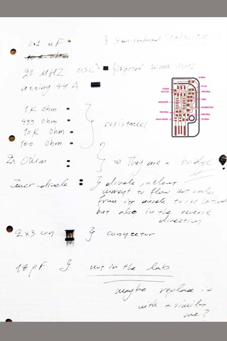
Being a clueless starter in the field of electronics led me to study more about its component. First , after conculting the suggested files and diagrams i collected all the components that were necessary to build a circuit. After making a list with the use and the characteristics of its one of this i studied the paths and the connections between them. Unfortunatelly, two of the components that i need in order to program my board are not available in our lab and we had to order them ;-(. An alternative way could be to replace them with something similar but since i am a beginner i chose to move in the safe way.
Soldering preparation//training
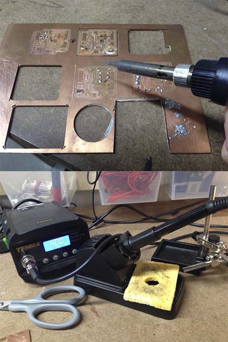
An old engravied attiny was used as a training plate. After being familiar with all the machines and equipment (soldering mashine, wire and some resistances, wet sponge in order to clean the bit of the warming pen), a lot of trials took place. The first group of trial had to do with melting the right amount of wire and transfering it to the plate in the right way. The secong group had to do with soldering the resistances in a right and clean way.
Final soldering
Being patient and not afraid to fail is the cornerstone of this step. After following some tutorial and mainly the directions of my instructor (who was very patient also with me this hard week....)i started to place the components by following the right sequence. First was placed the microcontroller ( the black box of my circuit as i call it ;-) ) and then the rest. It is essential to place the components at the right directions and agian, after the instructions of my instructor i was able to understand and read on the them their right side.
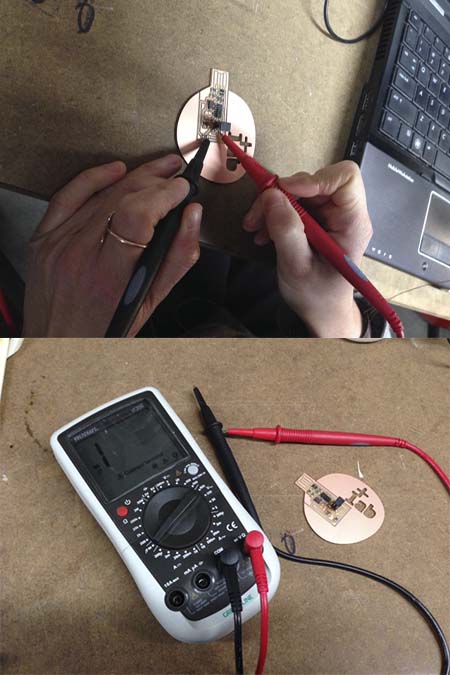
Checking the flow
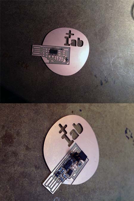
While waiting for the last components to arrive at the lab, i had to check the flow of my circuit and of the components were connected with each other. Following the connecting paths which were engraved on the attiny by testing the electricity flow on the poles of the two components,seemed that all the paths were working apart from one. The reason for this disfunctionality was the wrong engravement of a very small path , probably because of lack of a proper resolution. The specific componet will ne removed and by using a cutter manually a path will be cut out.
Red light
When the last component arrived ( 18 pf capasitor) it was placed with the same techique to the board. The wrong path (milled wrong from the roland mill machine) was cut and there is not longer a connection between the two components. The whole board was checked again and a mistake was found to one of the connections of the microcontroller. With the help and the support of my instructor Lorenzo, we placed two small wires in order to connect the appropriate paths since the copper path was lost in my attemp to resolder it.
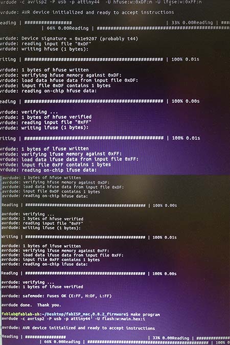
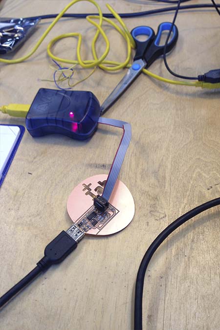
Programming
This was the hardest part since the red light was insisting even after the replacement of the microcontroller's connections. The computer was not able to regogninse the usb and i had to download the write drivers. With the right drivers the ISP's light chenged into green. The programming was occured in Ubuntu by following the fab academies's tutorials.
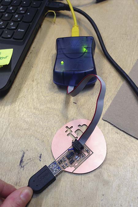
Green light
Brian's effective ISP
Finally, after having programmed the ISP in the correct way i still had problems with connecting Valentine's design with the microcontroller. After having a talk with Bas, he proposed to create another ISP and this time based on Brian's design. The procedure which was followed was exactly the same as before with the only difference that this one works perfectly!
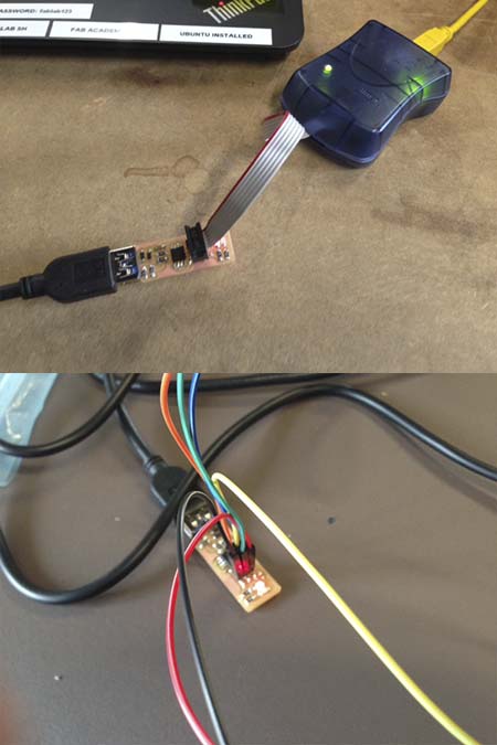
My ISP in action
Unfortunatelly, i only managed to use my fabISP during this week since i really tried to program with it the rest of the weeks but there was always the same error: please double check your connections. It seems that the problem was in the connection with my boards. Nevertheless, it worked perfectly the first time after programming. Since i spend a lot of time in this week by making two different fabISPS (the one of Valentine first and the one of Brian) i decided to continue with arduino as ISP.
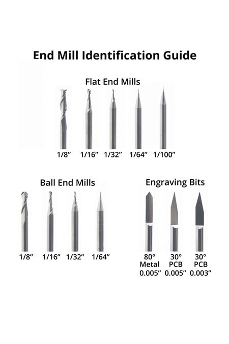
Bits information
Before i finish the documentation of this week i think that is essential to add a picture of the different bits that a roland milling mashine is working with. Until now i worked with a 1/64 inch bot for engraving and with a 1/32 bit for outline cutting.
Technical specifications//
HOW I MODIFIED THE PNG FILE INTO A PERSONAL ONE IN ILLUSTRATOR/INSKAPE // Step 1_ import the png file into illustrator with the place button. Step 2_ Image the bitmap with the image trace button. I propose the silouette option since we want a b&w result. Step 3_ expand the image. Step 4_ break the compound path and separate the black background(and delete it after) from the traces. Step 5_ Design the outline you wish and add any text who also want. Step 6_ select the nes outline and the traces and create a compound path. This is your traces image! Step 7_ Copy paste the traces image and then break the compound path once again. This time delete the traces and keep the outline filled with black color. Afterwards, copy and paste in place the black outline and change the fill into white. Then, minimize the white plane 0,2 mm. Export the file with a ppd of 1000 dpi. In the end you should have two png files, one with the traces and one with the outline.
FAB MODULES//TRACES PNG//Step 1_ import the trace image. Step 2_ output formal- rolland mil. Step 3_ process PCB traces (1/64). Step 3_ input dpi 1000. Step 4_ Input- SRM 20 , speed 4 and x0, y0 ,z0 turned to 0. Step 4_ process- tool diameter (mm) 0,3. Step 5_ Calculate button. Check the calculated diagram if all the traces are depicted as the png file. Step 6_ Save the file in rml and is ready to be milled.
FAB MODULES//OUTLINEs PNG//Step 1_ import the outline image. Step 2_ output formal- rolland mil. Step 3_ process PCB outlines (1/32). Step 3_ input dpi 1000. Step 4_ Input- SRM 20 , speed 4 and x0, y0 ,z0 turned to 0. Step 4_ Calculate button. Check the calculated diagram if all the outlines are depicted as the png file. Step 6_ Save the file in rml and is ready to be milled.
ROLLAND MILLING MASHINE//Step 1_ Open the milling software and the mashine by the on/off button. Step 2_ Unscrew the four screws of the plate and remove the base. Stick with a double side tape a copper plate on the base and screw it back in the mashine. Be careful that the copper plate is completly flat. Step 3_ Place the right bit for the traces. A 1/64 inch bit. Step 4_ Back to the software, move the bit with the x,y,z button to your wished x(0), y(0). Push the set button and do the same for the z axis after bringing the bit very closed to the copper plate and let it fall gently on it. Finally, raise the bit cause when the procedure will start the bit will move automatically and this will destroy and break it. Step 5_ Push the cut button and load the traces rml file. Press the output file and keep a close eye to the milling mashine. Step 6_ when the procedure is over remove the board and clean the mashine from the copper dust. Step 7_the procedure for the outline file is exactly the same with the only difference that the bit should changed into a 1/32fn inch bit. The change of the bit happens by unscrewing the bit from the mashine and placing back the right one. Step 8_ Press move to x,y axis and set again the new z axis as described before.
Conclusions//
The conclusions of this week are focus around the patience and the love for the detail that someone has to have in order to learn about electronics. The best advice is not to mimitise something but to study every detail and every aspect. Inthe end, electronics are like mathematics.